+420 54114 9207 |
  info@czechnanolab.cz
+420 54114 9207 | info@czechnanolab.cz
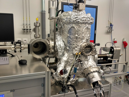
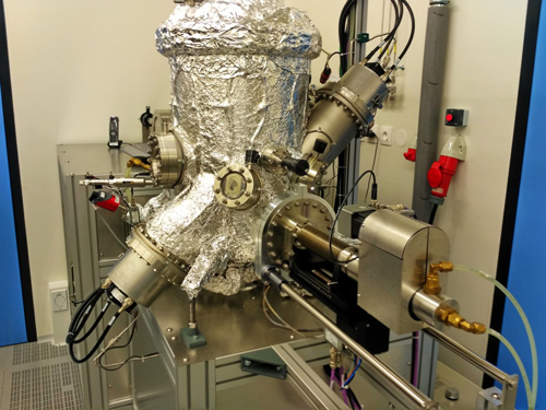
UHV sputter deposition system is equipped with two RFICP Kaufman ion-beam sources (KRI®) with 4 cm diameter grids (3-grid primary and 2-grid assisted/secondary) and charge neutralizer (LFN 2000 - KRI®). This setup is suitable for Ion-beam sputter deposition, Ion-beam assisted deposition, reactive sputter deposition with nitrogen and in-situ initial/continual substrate (pre-)cleaning. Etching (ion-milling) is not possible due to undesirable chamber and targets contamination.
Thin films are outstanding with their low surface roughness, residual stress control, crystal quality and purity. These properties make these layers appropriate i.e. for MEMS, optical applications or electrochemistry. Important parameters are listed in following table.
The system is mainly aimed at the preparation of CMOS compatible materials. Due to contamination risks a thorough discussion with the instrument guarantee is required before processing any samples.
| Base pressure | 1.2 x 10⁻⁸ mbar |
|---|---|
| Process pressure | 10−5 – 10−4 mbar |
| 5*10−5 Radiation heater | Up to 350 °C (real. temp. on substrate) |
| Available targets | Ti, Al, W, Hf, Ta, Zr |
| Gases | Argon (7.0), Nitrogen (7.0) |
| Deposition rate | 0.03 – 1.50 Å/s (based on material) |
| Beam voltage | 100 – 1200 V |
| Beam current | 5 – 120 mA |
| Wafer technology | 1 – 4 inch |